Günter G. Hoffmann,a,* Marcos Ghislandia,b and Gijsbertus de Witha
aDepartment of Chemical Engineering and Chemistry, Laboratory of Materials and Interface Chemistry (SMG), Eindhoven University of Technology, PO Box 513, 5600 MB Eindhoven, The Netherlands. E-mail: [email protected]
bCETENE–Center for Strategic Technologies of the Northeast, Av. Prof. Luiz Freire 1 (CDU), Recife–PE, 50740-540, Brazil
Introduction
Single-walled carbon nanotubes (SWCNTs)1 and graphene2 have received tremendous research attention during the last few years. Both allotropes of carbon have matchless mechanical and electrical properties. The extraordinary tensile strength of SWCNTs ranges from 13 GPa to 126 GPa (much higher than of stainless steel with 0.38 GPa to 1.55 GPa and of Kevlar® with 3.6 GPa to 3.8 GPa); the strength of graphene is also about 100 times that of steel. This makes these materials very attractive to be used as fillers in polymer composites and thereby increase the polymer’s strength and electrical conductivity.3,4 The excellent electrical conductivity of graphene makes a number of enhanced applications in electronics possible, for example, touch screens, field effect transistors and a large range of novel sensors of many kinds. Metallic SWCNTs can, theoretically, carry a current of 4 × 10⁹ A cm–2, which means that they conduct current about a thousand times better than copper. SWCNTs have a high thermal conductivity value of 3500 W m–1 K–1 along the axis of the tube, compared to 385 Wm–1 K–1 of copper. The thermal conductivity of graphene is even more impressive, with a measured value of 5000 Wm–1 K–1.
A SWCNT can be considered as a narrow sheet of graphene that has been rolled and fused. This is also apparent from the Raman spectrum:5,6 most features can be found in the spectra of both allotropes. The G-line, attributed to C–C stretching vibrations and named after its occurrence in graphite at 1582 cm–1, is split into two components in CNTs: the G+-line at 1590 cm–1, which is attributed to the stretching along the axis of the nanotube (longitudinal phonon mode) and the G–-line at 1570 cm–1, which arises from the transversal mode of the C–C stretching. The D-line at ~1350 cm–1 is only found if there are defects in the sample, so it is used to judge the quality of the material. In graphene it can also be used to detect the edges of the sheets, as these are considered “defects” in an infinite graphene sheet. The G¢- or 2D-band at 2700 cm–1 is the first overtone of the D-band and can be used to analyse the number of graphene layers in a graphitic sample using its Raman shift and the 2D-/G-band intensity ratio. The radial breathing mode (RBM, at 100 cm–1 to 500 cm–1), which is a C–C bond-stretching mode that moves all carbon atoms radially out, can, of course, only be observed from the tubes. As its wavenumber is inversely proportional to the tube’s diameter, it can be advantageously used to analyse a sample’s content of tubes with different diameters.
Tip-enhanced Raman spectroscopy (TERS)
Raman spectroscopy and infrared spectroscopy are complementary techniques for the qualitative and quantitative analysis of materials6,7 which, in addition to chemical composition, yield a lot of useful information including crystallinity and other properties of the sample under test. In the form of confocal Raman spectroscopy and infrared microscopy, they can also be used to spatially map the sample; the former being the higher spatial resolution technique. Due to physical limitations, the resolution is limited to 0.2–1 µm, depending upon the wavelength of the Raman spectroscopy excitation laser used. Using a “trick”, this limit may be overcome: in the case of Raman spectroscopy, a noble metal tip is placed at the focus of a confocal Raman spectrometer. The resulting technique is therefore called tip-enhanced Raman spectroscopy (TERS) in the case of a stationary sample, or tip-enhanced Raman mapping (TERM), for the case of a scanned sample. Using TERM, carbon allotrope samples can be analysed with high spatial resolution.8
The basic TERS experimental set-up for transparent samples is illustrated in Figure 1. Using a high numerical aperture (NA) microscope objective (of, for example, an inverted microscope), a laser beam is focused onto a sample. The sample can be moved in both the x- and y-directions by a high precision piezo sample stage. A very sharp needle (radius at tip ~30 nm), etched electrochemically from a thin gold wire, is attached to a miniature quartz tuning fork. By means of a second x–y-scanner in an atomic force microscope (AFM) shear force head, the gold tip is placed with high accuracy at the exact centre of the laser focus. Feedback from the tuning fork, vibrating at its resonance frequency, is used to keep the gold tip at a constant distance to the sample with a piezo z-scanner. The gold tip amplifies the electromagnetic field at its apex, resulting in a drastically enhanced Raman spectrum. The enhancement factor reaches 20,000 in the case of SWCNTs, if one is also taking the reduced area into account. The Raman light is collected by the same microscope objective used for the focusing of the laser beam and fed into a normal Raman spectrometer for analysis.
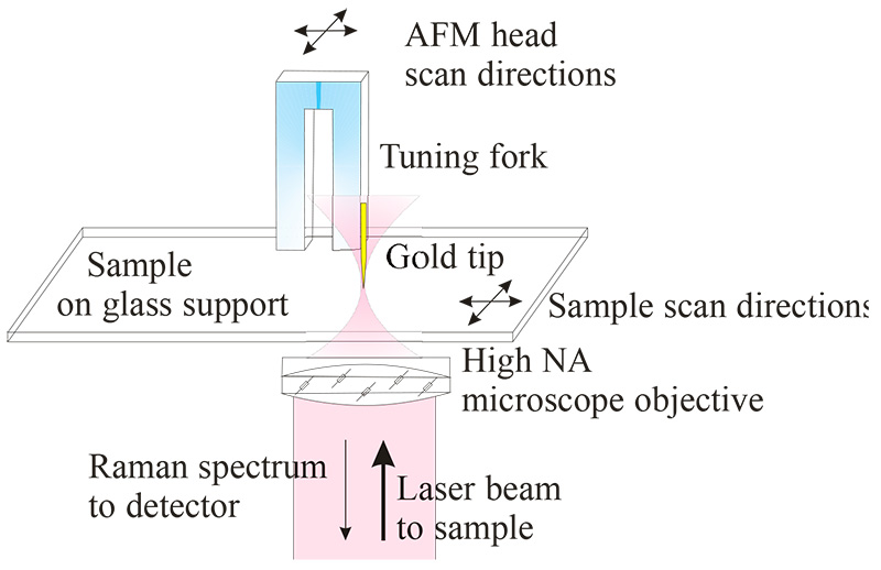
Figure 1. Basic TERS experiment, showing the measurement of a transparent sample on a thin glass support. A laser beam (from below) is focused by a high numerical aperture objective onto the sample. In the centre of the focus, a sharp gold tip, attached to a vibrating tuning fork, is placed. The distance of the tip is kept constant by a feedback loop to a piezo and the mapping is done by a high precision xy-stage. The enhanced Raman spectrum is collected by the objective and fed into the spectrometer.
TERM of single-walled carbon nanotubes
Figure 2 shows a comparison of a confocal Raman mapping to a TERM on a small bundle of single-walled carbon nanotubes.9 In principle, each line in the tip-enhanced Raman spectrum can be used for mapping, but the lower the intensity of the Raman line, the lower the signal-to-noise ratio in the map. In the figure, the three principal Raman lines of SWCNTs have been used for the mapping: RBM (row A), D-line (row B), and G-line (row C). The images labelled I show the confocal Raman mapping, those labelled II the TERM and those labelled III are showing cross-sections indicated by the white lines in column II. Clearly, the 10-fold increase in resolution from confocal to tip-enhanced Raman spectroscopy can be seen. A Gaussian fit to the cross-sections in III shows a resolution of 35 nm. The arrows denoted E® show the direction of polarisation of the excitation laser.
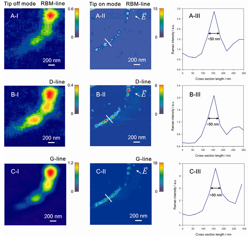
Figure 2. Comparison of confocal Raman mapping (column I) and TERM (column II) of a bundle of single-walled carbon nanotubes, using the RBM-line (A), the D-line (B) and the G-line (C). Column III shows cross-sections indicated by the white lines in column II [reproduced by permission from: S.S. Kharintsev, G.G. Hoffmann, P.S. Dorozhkin, G. de With and J. Loos, Nanotechnology 18, 315502 (2007). © 2007 IOP].
TERM of graphene
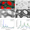
Figure 3 shows the experiments on a graphene sample10 which was grown by chemical vapour deposition (CVD) on nickel. After etching away the substrate, the sample was transferred to a thin microscope cover glass, where a confocal Raman map (a) was recorded using the shift position of the 2D line for mapping. The graphene area, surrounded by multiple layer material, could be identified as a flat area in the atomic force microscope’s phase image (b). A higher resolution Raman map could be obtained using TERS. Using the intensity of the 2D Raman band, an image (c) of the clearly defined graphene area could be obtained. If, in the TERS experiment, the shift position is again used for the mapping (d), the image shows more details: the graphene area is surrounded by a borderline. We can now pick special places from 1 to 4, where different spectra can be measured.
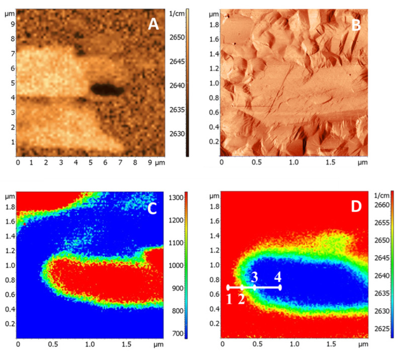
Figure 3. (a) Confocal Raman mapping of graphene (black dot)/graphite grown by CVD; (b) AFM phase image of graphene (flat region) area identified by Raman; (c) TER mapping showing intensity of the 2D-band for the selected area; (d) TER mapping showing shift position of the 2D-band [reproduced by permission from M. Ghislandi, G.G. Hoffmann, E. Tkalya, L. Xue and G. de With, Appl. Spectrosc. Rev. 47, 371 (2012).]
Figure 4 shows the Raman spectra that were taken at the positions shown in part (d) of Figure 3. At point 4 (blue curve) we measure a pure graphene spectrum, easily recognised by the 2D-band position and the low G- to 2D-band intensity ratio. Point 3 (green curve) corresponds to the edge of the graphene area: a D-peak appears. Moving further, to point 2 (yellow curve), more than one graphene layer can be detected from the breadth and the position of the 2D-band also the D-band increases. Finally, a graphite spectrum with high G- to 2D-band intensity ratio was acquired at point 1 (red curve).
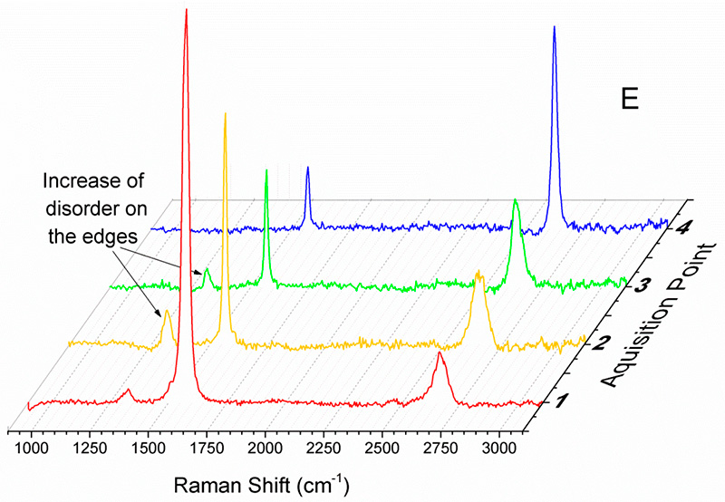
Figure 4. Raman spectra corresponding to points selected in Figure 3(d).
Conclusion
Tip-enhanced Raman spectroscopy (TERS) and tip-enhanced Raman mapping (TERM) can be used advantageously to investigate the carbon allotropes graphene and single-walled carbon nanotubes, with a spatial resolution in the nanometre range. Even the localisation of defects in one single sheet or tube is possible, with a spatial resolution of ~35 nm.
Acknowledgements
This work is part of the Research Program of the Dutch Polymer Institute (DPI), Eindhoven, The Netherlands, projects #648, #692 and #756.
References
- M.M. Shokrieh and R. Rafiee, “A review of the mechanical properties of isolated carbon nanotubes and carbon nanotube composites,” Mech. Compos. Mater. 46(2), 155 (2010). https://doi.org/10.1007/s11029-010-9135-0
- A.K. Geim and K.S. Novoselov, “The rise of graphene,” Nat. Mater. 6(3), 183 (2007). https://doi.org/10.1038/nmat1849
- M.F.L. De Volder, S.H. Tawfick, R.H. Baughman and A.J. Hart, “Carbon nanotubes: present and future commercial applications,” Science 339(6119), 535 (2013). https://doi.org/10.1126/science.1222453
- X. Huang, X.Y. Qi, F. Boey and H. Zhang, “Graphene-based composites,” Chem. Soc. Rev. 41(2), 666 (2012). https://doi.org/10.1039/C1CS15078B
- M.S. Dresselhaus, G. Dresselhaus, R. Saito and A. Jorio, “Raman spectroscopy of carbon nanotubes,” Phys. Rep. 409(2), 47 (2005).https://doi.org/10.1016/j.physrep.2004.10.006
- M.S. Dresselhaus, A. Jorio and R. Saito, “Characterizing graphene, graphite, and carbon nanotubes by Raman spectroscopy,” Annu. Rev. Cond. Mat. Phys. 1, 89 (2010). https://doi.org/10.1146/annurev-conmatphys-070909-103919
- G.G. Hoffmann, L. Xue, J. Loos and G. de With, “High-resolution tip-enhanced Raman mapping,” Macromol. Symp. 305(1), 26 (2011). https://doi.org/10.1002/masy.201000138
- G.G. Hoffmann, G. de With and J. Loos, “Micro-Raman and tip-enhanced Raman spectroscopy of carbon allotropes,” Macromol. Symp. 265, 1 (2008). https://doi.org/10.1002/masy.200850501
- S.S. Kharintsev, G.G. Hoffmann, P.S. Dorozhkin, G. de With and J. Loos, “Atomic force and shear force based tip-enhanced Raman spectroscopy and imaging,” Nanotechnology 18(31), 315502 (2007). https://doi.org/10.1088/0957-4484/18/31/315502
- M. Ghislandi, G.G. Hoffmann, E. Tkalya, L. J. Xue and G. de With, “Tip-enhanced Raman spectroscopy and mapping of graphene sheets,” Appl. Spectrosc. Rev. 47(5), 371 (2012). https://doi.org/10.1080/05704928.2012.666773

